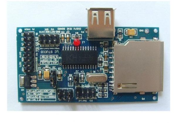
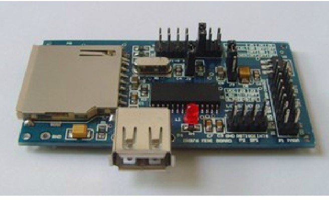
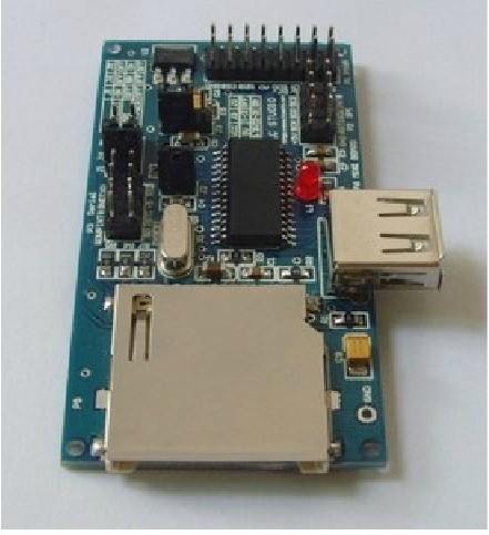
评估板中的主要器件U1 是CH376S 芯片,但是图中有些信号是以CH375 或者CH374 命名的。
The main devices in the U1 evaluation board is CH376S chip, but in some signal is CH375 or CH374 name.
晶体X1 为标准12MHz,USB 主机比USB设备要求更高的频率精确度,X1 的误差要求小于0.4‰,普通的12MHz 晶体基本上可以满足要求。强烈建议缩短相关引线的长度,以减少干扰。
Crystals of X1 as the standard 12MHz, USB host than USB equipment required frequency accuracy higher, X1 error is less than 0.4 ‰, 12MHz crystal can basically meet the requirements of general. Strongly recommended to shorten the lead length, to reduce interference.
电容C4 用于内部电源节点退耦从而降低USB 传输过程中的EMI,容量为4700pF 到0.1uF,可以选用普通的103 贴片电容0.01uF。
Capacitor C4 for internal power supply node decoupled to reduce USB transmission process of EMI, the capacity is 4700pF to 0.1uF, you can choose 103 SMD capacitors 0.01uF ordinary.
P4 是USB 端口,既可以用于USB HOST主机方式,也可以用于USB DEVICE设备方式,电阻R1 用于限制输出给外部USB设备的电流,避免在U 盘等USB设备刚插入时造成电源电压的短时间下降,甚至引起CH376或者单片机非正常复位或者内部RAM 数据错误。如果是USB 外置硬盘,那么应该将电阻R1 换成直流电阻较小的电感,或者另外用一组5V 电源直接提供更大的工作电流(500mA 以上)给外置硬盘。另外,USB-HOST插座的电源退耦电容C9的容量不能太小,容量大些(应该大于100μF)可以减少在USB 设备刚插入时的电源电压的波动。
P4 is a USB port, which can be used for USB HOST host mode, can also be used for USB DEVICE devices, R1 for the current limit resistor output to external USB device, avoid the short time caused by power supply voltage in the U plate, USB equipment was inserted decline, and even cause the singlechip CH376 or abnormal reset or internal RAM data error. If it is a USB drive, it should be changed into the inductor resistance R1 DC resistance is small, or by a group of 5V power supply directly provide more current (above 500mA) to an external hard disk. In addition, the power supply socket USB-HOST decoupling capacitor C9 capacity can not be too small, large capacity (should be larger than 100 μ F) can reduce the supply voltage in the USB equipment is just inserted when fluctuation
P5 是SD 卡插座,可以接触标准尺寸的SD 卡,其它规格的SD 卡可以需要另加转换座。电阻R3用于限制输出给外部SD 卡的电流,避免在SD 卡刚插入时造成电源电压的短时间下降。
P5 is a SD card socket, can reach the standard size of the SD card, the other specifications of the SD card can need additional conversion base. For the current limiting resistor R3 is output to the external SD card, avoid the short time caused by power supply voltage in SD Kagan is inserted down.
P1 是8 位并口的信号端口,用于连接单片机的并口,并口的必要信号包括D0-D7、A0、RD#、WR#、CS#以及GND,而INT#是可选的。
P1 is a 8 bit parallel port used to connect the signal, single chip microcomputer parallel port, the necessary signal parallel including D0-D7, A0, RD#, WR#, CS# and GND, but the INT# is optional.
P2 是SPI 串口的信号端口,用于连接单片机的SPI 接口,SPI 的必要信号包括SCS、SCK、SDI、SDO 以及GND,而INT#是可选的。
P2 is a signal port SPI serial port, SPI interface used to connect the chip, the necessary signal SPI including SCS, SCK, SDI, SDO and GND, but the INT# is optional.
P3 是异步串口的信号端口,用于连接单片机的异步串口,异步串口的必要信号包括RXD、TXD 以及GND,而INT#是可选的。P3 同时提供了SD 卡的写保护SDWP 和插拔状态SDINSERT 信号线。
P3 is a signal port asynchronous serial port asynchronous serial port, used for connecting one of the microcontroller, the necessary signal asynchronous serial interface including RXD, TXD and GND, but the INT# is optional. P3 also provides the write protect SDWP and plug the SDINSERT signal line SD card.
上述P1、P2、P3 通讯端口,还可以从外部向本评估板提供5V 电源,以及向CH376 的RSTI 引脚提供可选的硬件复位信号,如果实际产品电路中有μP 监控电路,那么应该为CH376和单片机提供同一个复位信号。注意,应该尽量缩短本评估板与单片机之间的信号线的长度,最长不能超过20cm,否则需要使用一个信号间隔一个地线的专用排线。
The P1, P2, P3 communication port, can also provide 5V power from the outside to the evaluation board, as well as to the CH376 RSTI pin provides a hardware reset signal is optional, if μ P monitoring circuit actual product circuit, it shall be provided with a reset signal for the CH376 and single chip microcomputer. Pay attention to, should try to shorten the signal line between the board and the evaluation of single length, the length of not more than 20cm, special cable or requires the use of a signal at intervals of one wire
J3 用于选择CH376 芯片工作电压,短接1-2 脚时为5V 电压,短接2-3 脚时为3.3V 电压。默认为5V 电压,但当单片机的工作电压等于或者低于3.3V 时,可以为CH376 选择3.3V 电压。当CH376芯片的工作电压为5V 时,J2 必须断开,当CH376 芯片的工作电压为3.3V 时,J2 必须短接。
J3 is used to select the CH376 chip voltage, short circuit 1-2 feet for the 5V voltage, short circuit to 3.3V voltage 2-3 pin. The default for 5V voltage, when the voltage is equal to or lower than the single chip 3.3V, can choose 3.3V voltage CH376. Working voltage when the CH376 chip 5V, J2 must be disconnected, the working voltage when the CH376 chip 3.3V, J2 must be short circuited.
J1、J5 和J6 用于在上电或者硬件复位后选择CH376 与单片机的通讯接口:
J1, J5 and J6 is used to select the communication interface of CH376 and single-chip microcomputer in hardware reset power on or after:
如果J1 短接、J5 断开、J6 断开,那么是8 位并口;
If the J1 short connection, J5 off, J6 off, so is a 8 bit parallel port;
如果J1 断开、J5 短接、J6 短接,那么是SPI 接口;
If the J1 is disconnected, J5 shortened, J6 shortened, so is the SPI interface;
如果J1 断开、J5 断开、J6 断开,那么是异步串口。
If the J1 off, J5 off, J6 off, so is the asynchronous serial port.
有些例子程序可能会用单片机的串口输出调试状态信息,如果需要显示这些监控信息,可以由将单片机串口经过RS232 电平转换后连接到计算机使用串口监控/调试工具软件查看。如果使用CH375评估板,那么可以将J2 连接到计算机串口;如果计算机没有串口,或者串口已经被其它设备占用,那么可以由USB 转串口芯片CH341 提供仿真串口。
Some examples of procedures may be debugging information using the serial output, if the need to display the monitoring information, can be the serial after RS232 level conversion and connected to a computer using a serial port monitoring / debugging tools to view. If you use the CH375 evaluation board, so J2 can be connected to the serial port of the computer; if the computer is not serial, or serial port has been occupied by other devices, you can USB to serial chip CH341 serial port emulation.
CH375 评估板内部器件工作于5V 电源电压时,必须加上电阻R0 并去掉3.3V 稳压器D4,工作于3.3V 电源电压时,必须加上稳压器D4 并去掉电阻R0。默认是5V 电源。
The CH375 evaluation board of internal components in supply voltage is 5V, must add the resistance R0 and remove the 3.3V regulator D4, works in the 3.3V power voltage regulator D4, must add and remove resistance R0. The default is 5V power supply.


